The military competition of artificial intelligence (AI) computing power continues to rise, and global basic facility investment is ushering in the largest wave of scale in history. However, AI industries are facing "a fundamentally high wall" in terms of data movement between processors. Because existing interconnected technologies that use copper wires are no longer able to effectively expand, further serving the millions of processors required for the new generation of AI. Against this backdrop, Celestial AIAI and OpenLight, a new company in Photonic Chips, are rapidly emerging, providing faster and lower power solutions to meet the needs of hyperscaler customers such as Amazon, Micro and Google.
Celestial AI has Tel.com and Samsung investment, locking servers to expand the market
In order to meet the market's demand for the next-generation AI-based infrastructure, Photonic Chip New Creation Company has received strong financial support and deepened its cooperation with foundry partners. Among them, Celestial AI received US$255 million from VentureTech Alliance and Samsung Catalyst Fund in August 2025, bringing its total fundraising amount to US$520 million. Celestial AI plans to use this new fund to strengthen its supply chain and deepen its relationship with OEM cooperation partners including NT$1.
In addition, OpenLight also collected $34 million in funds in August, with investors including Juniper Networks (now part of HPE) and Lam Capital, the corporate investment division of Lam Research. OpenLight is also preparing to use new capital to expand its process design kit (PDK) data for active and passive photonic components, and has been manufactured by the foundry manufacturer Tower Semiconductor through related components.
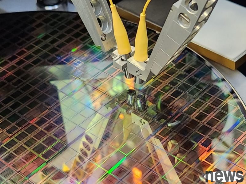
Judging from the current progress, Celestial AI plans to start selling its first batch of chips from mid to second half of 2026. Because of its focus on the server "scale-up" network, accounting for 85% of data traffic in the data center, the sales volume of the directional expansion exceeds the scale-out exchanger based on copper wires from 2025. The core technology of Celestial AI is Photonic Fabric, which provides an optical expansion network from processor packaging internal chips to chips, or servers across data center racks to servers. Moreover, Photonic Fabric is significantly better than NVIDIA's (Nvidia)'s NVLink interconnect technology, and Celestial AI is also using its proprietary Optical Memory Interface Bridge (OMIB) as an alternative to NVLink.
Celestial AI Explanation, OMIB is an advanced packaging, similar to Intel EMIB, TECHNOLOGY CoWoS and Samsung IQE, providing photon connection between wafers and wafers. The transmission and reception of Celestial AI control circuits are carried out using trunk 4 and 5 nanometer chips, and the speed and efficiency are comparable to that of Nvidia. The operation is completed in 600~700 ncs. The Celestial AI can be completed in 100~200 ncs, and the power consumption is extremely low, about 2.8 picojoules per bit.
In addition to the above patented technologies, Celestial AI's technical breakthroughs include the use of electrical absorption modulators (EAMs) to control the intensity of the laser beam, rather than the use of heat-sensitive micro-rings, which use EAMs to apply the electric field to adjust the absorption of the light. This design allows Celestial AI to place optical I/O anywhere on the wafer, solving the challenges of electromagnetary interference (EMI) signal integrity when connecting high-density interconnections within large wafers. Celestial AI is currently in the tapping out stage, and after formal production, it will place the world's first large chip to place optical I/O in the center of the chip.
In addition, Celestial AI is also developing a unified memory space architecture. The company placed two HBM3e controllers on the south side of the wafer and four DDR controllers on both sides of the wafer to handle eight DDR DIMMs. Through software, HBM can be used as a cache for DDR. Because it can allow any processor to read any memory location and store TB-level deep learning recommendation models (DLRMs) locally, thus hiding the memory access delay of DRAM, this has become another innovative technology for Celestial AI.
Celestial AI plans to integrate its IP into customers' dies in the future, or provide optical chiplets for customers to package. These optical small wafers contain EIC (embedded intermediary layer loading) technology, an new packaging technology that integrates small wafers into multi-layer and wafer-like packaging at a cost lower than traditional 3D ICs..
OpenLight uses phosphating technology to help customers develop their own chips by providing information. In terms of OpenLight's development, the company plans to start production of related products for its first batch of customers by the end of 2025. The main advantage of OpenLight is the use of indium phosphide technology to integrate lasers onto the chip through abnormal integration. OpenLight notes that some of the current considerable customers are very interested in applying phosphides to co-packaged optical components (CPOs). Therefore, OpenLight has successfully demonstrated a 400 Gbps modulator that uses phosphide, and its 200 Gbps modulator achieves an extremely low power consumption of about 1.5 picojoules per bit. This ability to be integrated by a different quality represents the power consumption per bit that is almost half as the voltage increases are small.
In fact, OpenLight is unique in the industry chain because it does not necessarily make chips for customers, but provides a set of component (PDK library) data to enable customers to design their own chips. OpenLight is working with Silicon (ISE), a subsidiary of chip packaging company ASE Holdings.
In order to directly challenge the NVLink market, Taiwan’s supply chain and new found its cooperation The current competition in the photonic chip field is becoming increasingly fierce, with other competitors including Ayar Labs, Lightmatter and China. Among them, in order to also aim to challenge the NVLink market, the company announced its new SuperPod cluster, which plans to connect up to 15,488 thriving NPUs in 2026 and operate them as a connected system.
As for, Lightmatter announced the Passage M1000 platform plan in March, which can provide 114 Tbps total optical bandwidth. The M1000 reference platform is a multi-veil active photon interposer for connecting large dies in 3D packaging. Lightmatter has partnered with GlobalFoundries and Amkor to start producing M1000-based customer designs.
In addition, the new quantum computing company PsiQuantum also uses standard 45-nanometer silicon nitride process to make photonic chips at Grofontein's New York Malta factory. Ayar Labs announced in September that it will cooperate with Alchip Technologies to combine Ayar's CPO technology and Shixin's professional design knowledge with advanced packaging technology from Taiwan Electric's COUPE (Compact Universal Photonic Engine).