According to the latest report from Goldman Sachs, China has lagged behind international peers for at least 20 years in the development of exposure technology in the semiconductor manufacturing key ring.
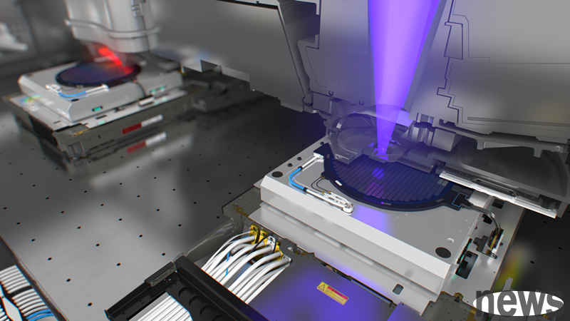
Report pointed out that this technology is not only an important period for several semiconductor manufacturing, but also the only bottle that hinders China's production of high-level chips. In this case, the advanced exposure machines manufactured by Dutch ASML, especially its extreme ultraviolet light (EUV) and high-value pore EUV exposure functions, build extremely small circuit patterns on the silicon wafer, thereby greatly improving chip performance. However, it is the supply of these cutting-edge equipment that has become a pain point in China.
At present, since ASM's exposure machine is still highly dependent on parts of original US products, the US government has been able to use this influence to restrict its sales to China. This ban has had a profound impact on China's science and technology industry. For example, China's science and technology manufacturer, which was sanctioned by the US government for its connection with its military, was unable to obtain chips from Taiwan Power Corporation, and was forced to seek support from China's SMIC. However, SMIC has not been exempted from it. In the same way, the restrictions on purchasing EUV chip manufacturing exposure machines mean that Chinese companies can only reach a maximum of 7 nanometers in chip manufacturing.
Goldman Sachs' report stated that even though SMIC can actually produce 7-nanometer-process chips, it is very likely that these 7-nanometer chips will still be produced through ASML's older deep ultraviolet (DUV) exposure machines, because China itself does not have the ability to make advanced exposure machines, because the core components of these devices are mainly from around the world, especially the United States and Europe.
Goldman Sachs' analysis clearly pointed out that exposure technology achieves the key role of precision circuit construction on the wafer, making it a decisive bottle in the wafer manufacturing process. At present, the world's leading chip manufacturers such as TECHNOLOG, can produce 3-nanometer chips on a large scale and are actively preparing to enter 2-nanometer technology. Opinion: Chinese exposure equipment manufacturers whose technical level is still at the 65-nanometer process relative to Chen.
Goldman Sachs' report also quoted data strongly, Dutch ASML has spent 20 years on research and development and capital expenditures of up to USD 40 billion in order to increase its exposure capacity from 65 nm to less than 3 nm. Taking into account China's current technical level and the large investment required, as well as the complex dependence of global supply chains, the foreign capital data is predicted contemporaneously that the possibility of Chinese companies increasing Western advanced technology in the short term is "very slim". This undoubtedly sets up huge obstacles for China to achieve self-sufficiency in the field of high-level chips.